

1
Checks as you work
Errors show up the moment you make them, not as a surprise when you finally remember the ERC button hidden in a menu.
// shorts · clearance · airwires · one-pin netsSchematic, layout and parts, plus the analysis that tells you what's wrong while it's still free to fix.
A board that comes back wrong costs weeks. PCBPA is full of analysis and visualizations built to catch the problem while it's still a few pixels.
Errors show up the moment you make them, not as a surprise when you finally remember the ERC button hidden in a menu.
// shorts · clearance · airwires · one-pin netsVoltage drop across every load and the spots where current crowds, so you widen the right trace.
// mV drop · A/mm² · trace heatingWatch the board heat up over time, including parts that only run in bursts, and boards with active cooling.
// duty cycles · still air · fansEvery signal net ranked against the FCC Class B limit, so you know which loop to tighten before the test lab does.
// FCC Class B · margin per netMark what a net carries: power, or a common digital signal from a list. You don't have to, but even a little information lets the analysis tools start working.
// USB · I²C · SPI · UART · power railsExport to SPICE for deeper analysis. And yes, you can plug PCBPA into an MCP if you like.
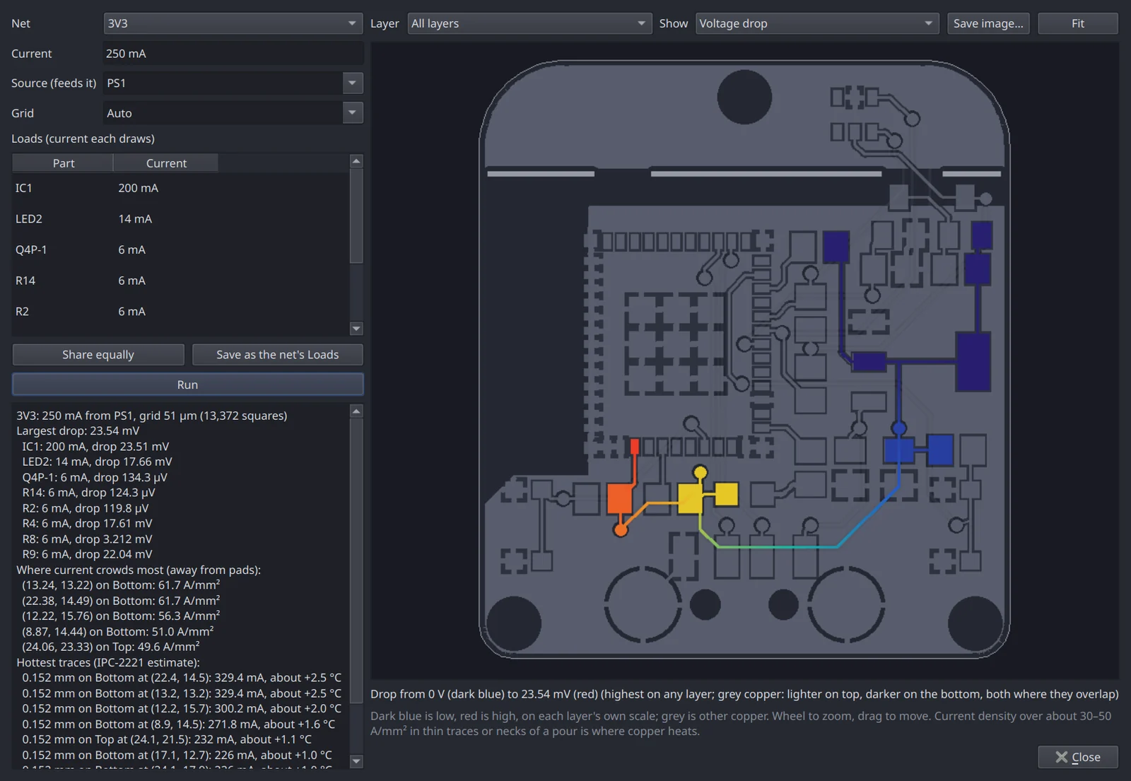
// SPICE export · MCPPick a net and its loads. PCBPA maps voltage drop across the copper, flags where current density gets high, and estimates how warm the thinnest traces run.
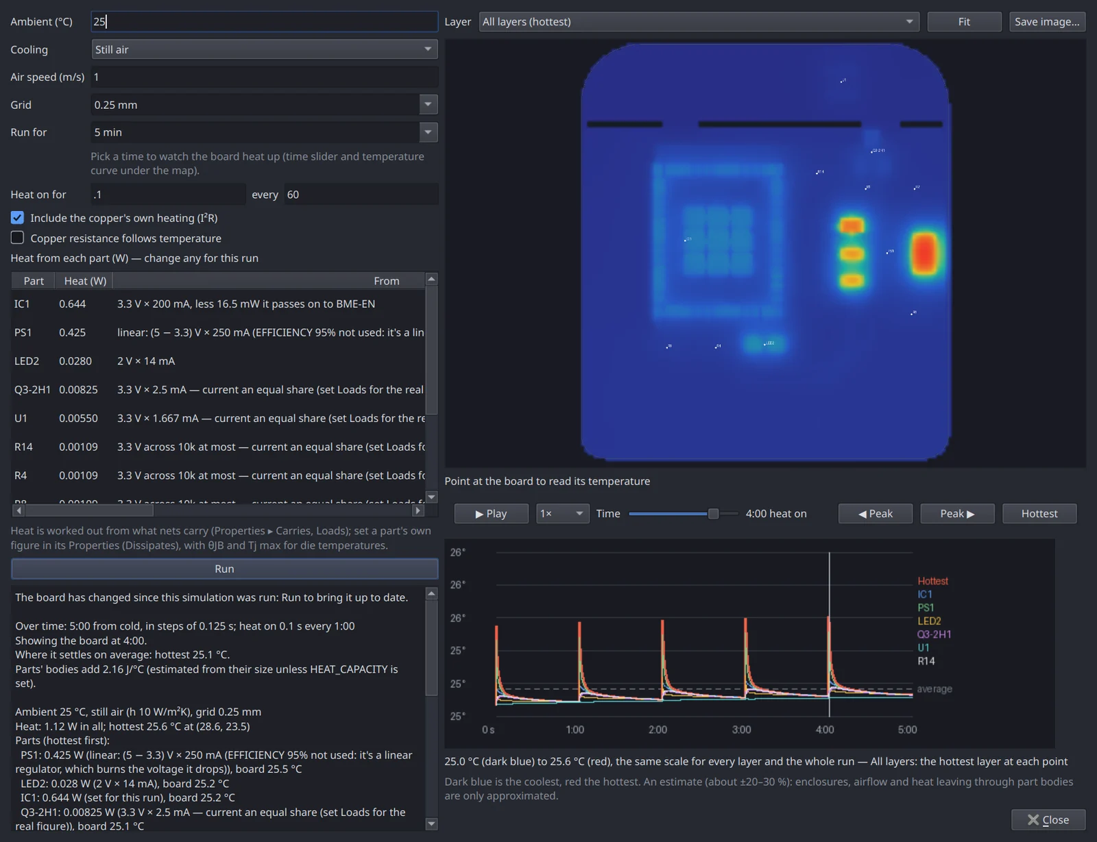
Set the ambient, the cooling and how often each part is busy. PCBPA steps the board through time and shows the hottest parts, layer by layer.
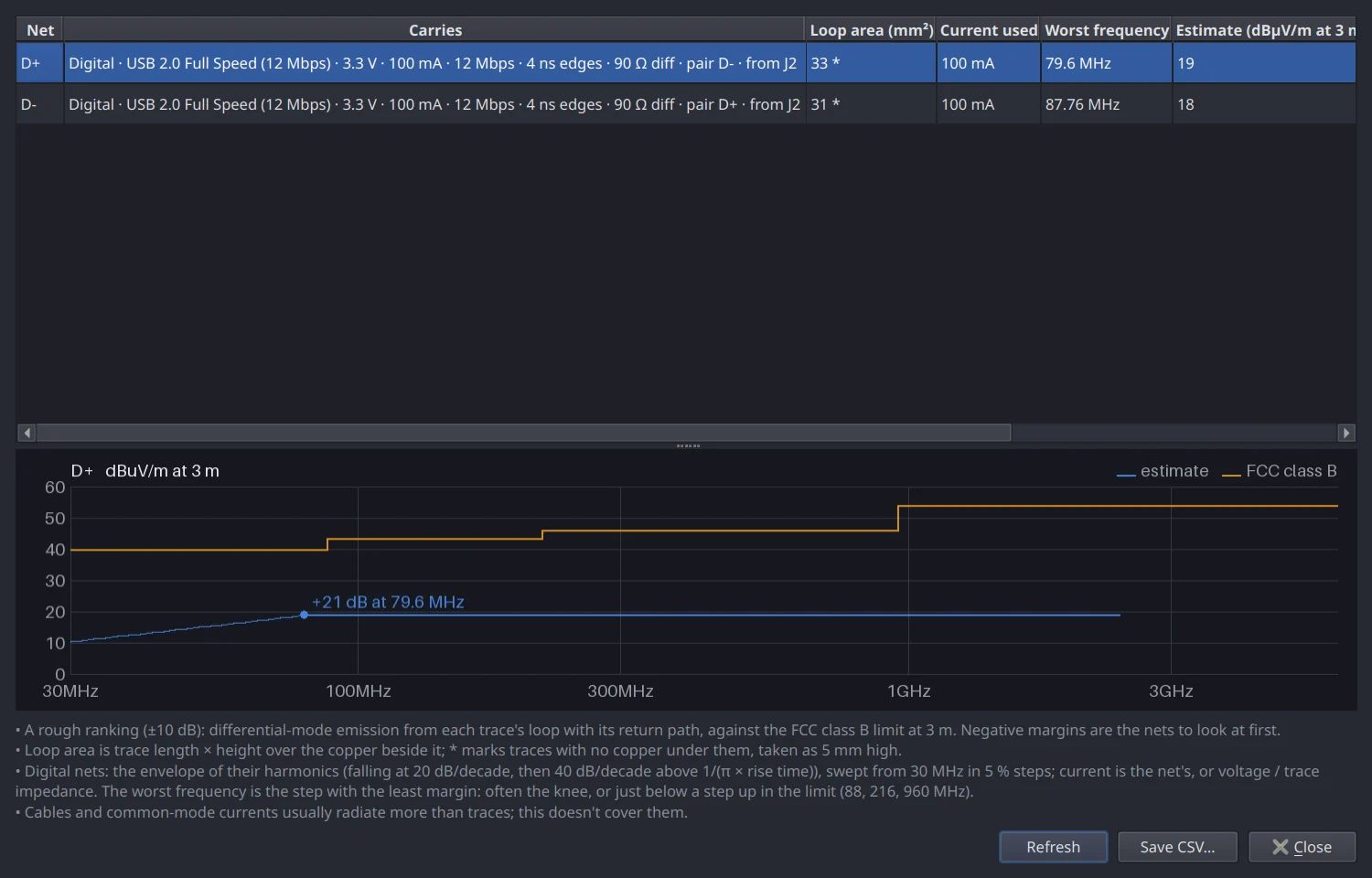
Loop area, edge rates and current for every signal net, swept against the FCC Class B limit. The nets with the least margin come first.
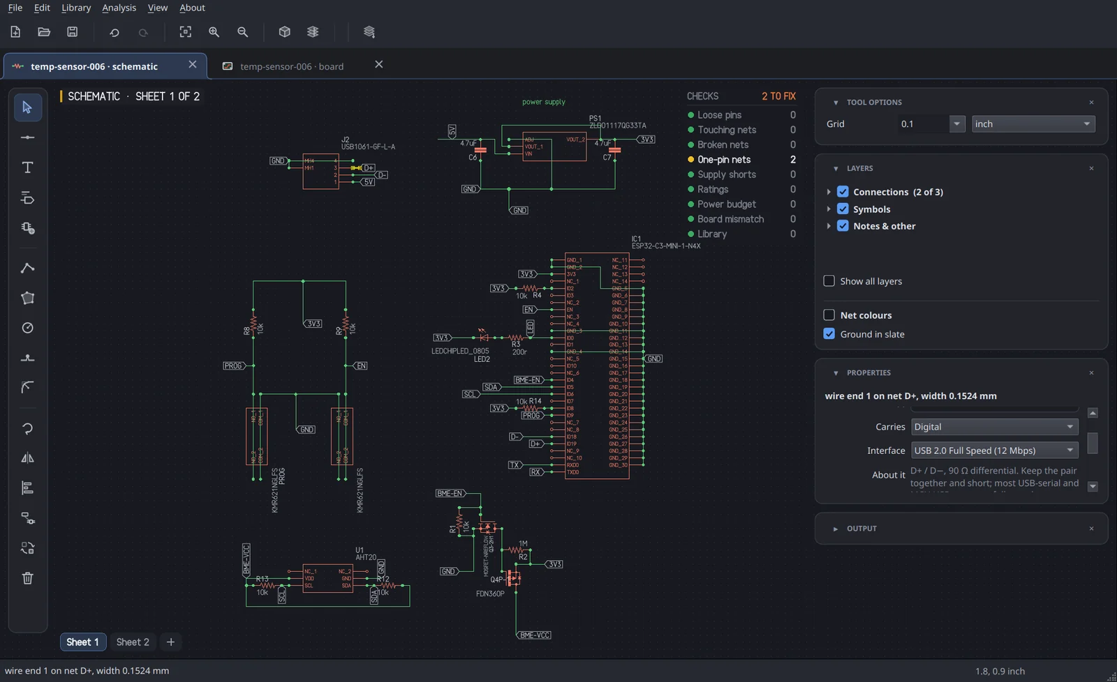
An improved schematic editor where every connection is obvious: you can see what's joined, what's touching by accident, and which pins are left hanging.
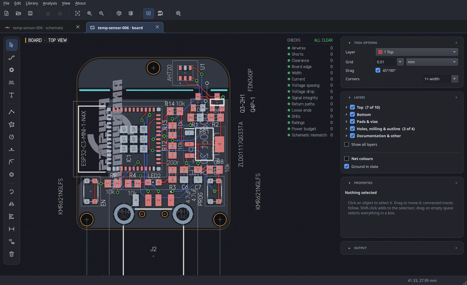
The board view is designed to be read, not deciphered, with tools for better component placement and cleaner board outlines built in.
Spin the assembled board around and check it fits before you order.
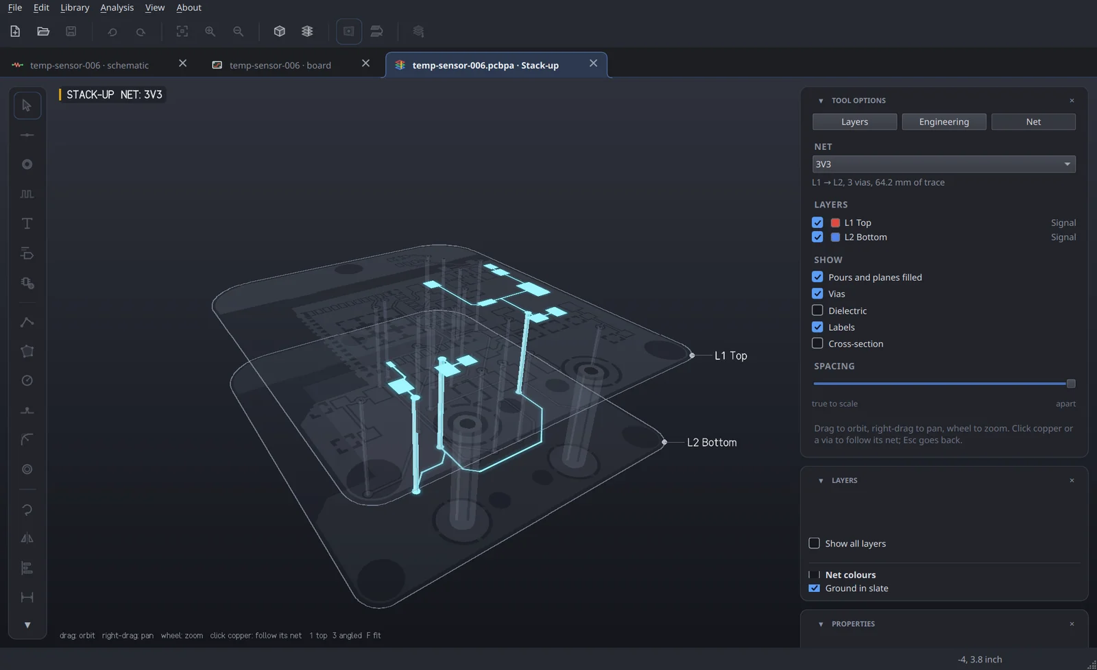
Pull the layers apart and follow a net from pad to via to pad, through every layer.
Step-and-repeat your board into a panel when you export, ready for the fab.
Click any copper or via and PCBPA lights up the whole net in 3D: every trace, every layer change, and how much copper it really is.
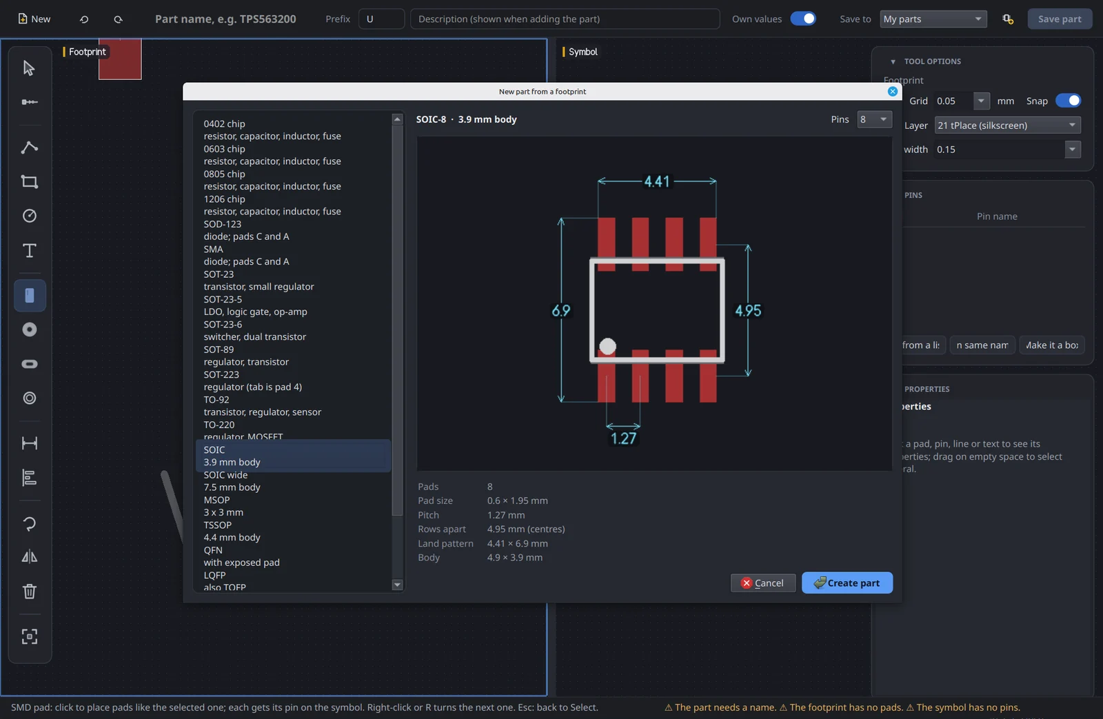
A parts library and a much easier parts editor. Pick a standard package (SOIC, QFN, SOT-23, 0603 and more), set the pin count, and the footprint is drawn for you.